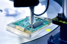
Initial understanding of PCB
1. What is PCB
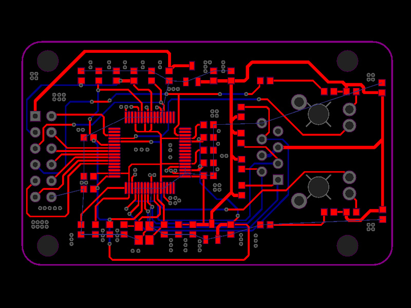
The full name of PCB is printed circuit board. It is an electronic device interconnection structure that uses processes such as printing and etching to deposit conductive materials (such as copper foil) in a patterned manner on an insulating substrate. It provides mechanical support and electrical connection paths for electronic components, and is the basic platform for functional integration and miniaturization of electronic systems. Through pre-designed circuit layout, PCB can ensure the accuracy and reliability of signal transmission, reduce wiring errors, improve production efficiency, and help simplify the assembly process and maintenance of electronic equipment.
Since American inventor Paul Eisler first applied printed circuits to radio manufacturing in the early 20th century, PCB technology has evolved from simplicity to complexity, from low density to high density, and from rigidity to flexibility. During World War II, the miniaturization and reliability requirements of military equipment for electronic equipment promoted the mass production and technological innovation of PCBs. Compared with the traditional point-to-point wiring method due to its low efficiency, poor reliability, large volume and other shortcomings, PCB has gradually emerged and eventually become popular in the electronics industry due to its efficient space utilization, excellent electrical performance and mass production characteristics. Establish dominance.
2. Basic structure of PCB
PCBs are usually made up of multiple layers of different materials. Let’s start with the core.
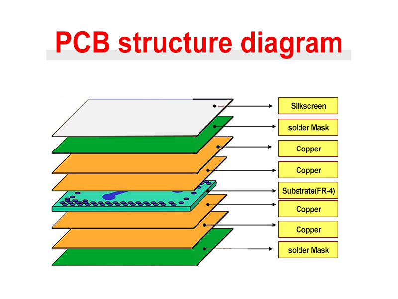
1. Substrate
The core part of PCB, usually made of FR-4 (glass fiber reinforced epoxy resin), PTFE (polytetrafluoroethylene), ceramic or metal, etc., to provide mechanical strength for the entire circuit board and electrical insulation.
2. Copper Foil Layers
As a conductive medium, copper foil is bonded to the substrate and formed into a predetermined circuit pattern through an etching process. Depending on the number of layers, PCBs can be divided into single-sided boards, double-sided boards and multi-layer boards. Multi-layer boards contain staggered signal layers, power/ground layers and internal electrical layers.
3. Prepregs
In the production process of multi-layer boards, prepreg is a semi-cured sheet material containing resin and fiberglass cloth, which is used to bond each layer of core boards and realize the interconnection of conductive vias.
4.Solder Mask
A protective coating covering non-welding areas, usually composed of photosensitive resin or thermosetting resin, to prevent bridging during welding and also plays a role in preventing corrosion and moisture.
5. Silkscreen
Also called the identification layer, it is used to print component symbols, text descriptions, positioning points and other information to facilitate assembly and maintenance.
The composition of PCB is not only reflected in the layering and complexity of the physical structure, but also in the deep integration of materials science and engineering technology. By continuing to develop high-performance, environmentally friendly PCB materials and optimizing circuit board design and production processes, we can effectively promote the miniaturization, lightweight and high-performance process of electronic equipment, and provide solid technology for the innovation and development of the electronic.
3. PCB types and applications
1.Single-sided PCB
Single-sided PCB is the most basic type of PCB. It has a conductive circuit layer on only one side and all components are concentrated on this side. Due to its simple structure and relatively low manufacturing cost, it is suitable for low-density, miniaturized and low-cost electronic products, such as simple remote controls, radios, etc.
2.Double-sided PCB
The double-sided board has conductive patterns laid on both sides, and the electrical connection between the two sides is achieved through via holes. Compared with single panels, double panels can effectively improve space utilization, support more complex wiring, and are widely used in various consumer electronics products, industrial control equipment, and some communication equipment.
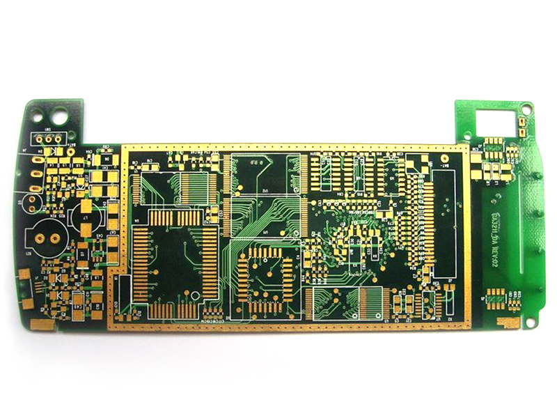
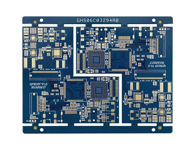
3.Multi-layer PCB
A multilayer board is made up of multiple double-sided boards stacked with insulating dielectric materials sandwiched in between, and interconnections between internal layers are achieved through via holes or buried blind holes. According to the number of layers, it can be divided into 4-layer boards, 6-layer boards, 8-layer boards and even ultra-high-density multi-layer boards with dozens of layers or more. Multilayer boards have higher circuit integration and signal transmission speed, and are often used in products with stringent performance requirements such as high-performance computer motherboards, servers, network equipment, medical equipment, and aerospace fields.
4. High Density Interconnect (HDI) PCB
High-density interconnection PCB is a PCB product that uses advanced technical means such as micro-blind buried vias, thin dielectric layers and fine lines to achieve high-density wiring. This type of PCB significantly improves the circuit layout capability per unit area, reduces signal delay, and optimizes electromagnetic compatibility. It is especially suitable for miniaturized and lightweight electronic products such as mobile communication equipment, smart phones, and tablet computers.
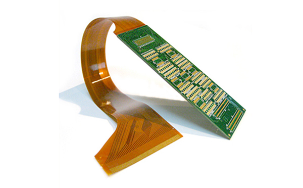
5. Flexible PCB
Flexible PCB is made of flexible polyimide film or other flexible substrates and can be bent and folded arbitrarily in three-dimensional space, which greatly enhances the design flexibility and space utilization efficiency of electronic products. FPC is widely used in portable electronic devices, wearable devices, automotive electronics, medical equipment and other fields.
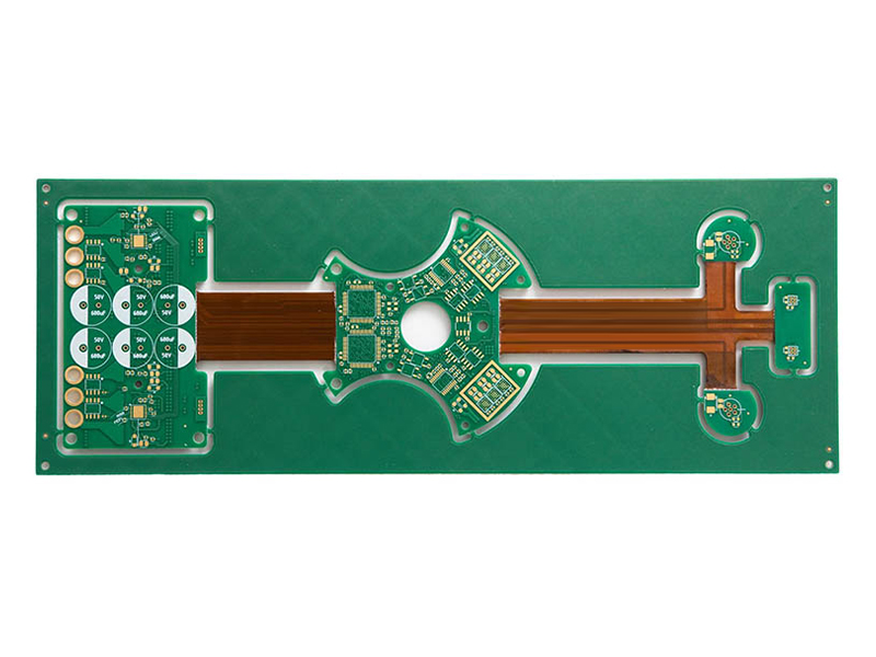
6. Rigid-Flex PCB (Rigid-Flex PCB)
Rigid-flexible PCB is a new type of PCB that combines the advantages of rigid PCB and flexible PCB. It not only retains the structural stability of rigid PCB, but also takes advantage of the three-dimensional spatial layout of flexible PCB. It is commonly found in precision electronic products such as aerospace, military equipment, high-end camera modules, and mobile phone camera modules.
4. PCB manufacturing process
1. Design PCB
Carry out system-level design based on product function, electrical performance, mechanical structure and other requirements, and clarify the required number of PCB layers, wiring density, signal integrity requirements, etc. Then use EDA (Electronic Design Automation) software to complete the PCB design and generate Gerber files and other pattern making materials. These files contain key information such as PCB circuit layout, pad position, and stack-up structure. When designing PCB, you need to consider the following two points:
Layout design: Reasonably arrange the location of components according to factors such as signal flow direction, electromagnetic compatibility, heat dissipation, and optimize power/ground network planning.
Wiring design: Follow the design rules and use automatic or manual methods for wire layout and routing to ensure the quality of high-speed signal transmission, reduce crosstalk, and meet safety spacing requirements.
2. Choose the right PCB material
Substrate selection: Select the appropriate copper-clad laminate material according to the design requirements, such as FR-4, polyimide, PTFE, etc., and consider its dielectric constant, heat resistance, dimensional stability, moisture absorption and other factors.
Conductor material: Determine the copper foil type (electrolytic copper or rolled copper), as well as copper thickness and surface treatment (OSP, ENIG, HASL, etc.) to ensure conductive performance and welding quality.
Solder mask and screen printing materials: Use solder mask materials that meet environmental requirements and have good adhesion and corrosion resistance, as well as clear and durable screen printing inks.
3. Graphic transfer
Make a film master: Make an accurate photomask or laser direct imaging template (i.e. “film”) based on the design file for subsequent graphic transfer.
Pattern exposure: Transfer the circuit pattern to the photosensitive film layer on the copper clad board through UV exposure or direct laser exposure.
Development and etching barrier layer: After water washing and development, a resist layer for the circuit pattern is formed to protect the copper foil at the corresponding position from being etched.
4. Subtractive method line production
Etching process: Chemical etching is used to remove the copper foil from unprotected areas to form the required conductive lines.
Film removal cleaning: remove the useless resist layer and clean the circuit board to ensure surface cleanliness.
5. Multi-layer board stacking and lamination
Inner layer alignment: For multi-layer PCB, the etched inner layer boards need to be accurately aligned and bonded according to the design requirements.
Interlayer positioning and hot pressing: Use high-temperature and high-pressure equipment to hot-press each layer together to form a stable laminated structure.
6. Mechanical processing
Drilling: Precisely drill through CNC drilling machines to complete the production of via holes, mounting holes and other mechanical structures to ensure the precise positioning and electrical interconnection of components.
Deburring and cleaning: Deburr the PCB after drilling to ensure smooth hole walls and reduce potential quality problems.
7. Electroplating process
Hole metallization: Perform chemical copper plating or electroplating copper process on the drilled holes to achieve conductive connections in the holes.
Outer layer circuit plating: thickening the exposed circuit to improve conductivity and welding reliability.
8. Surface treatment and solder mask coating
Silk screen marking: Print component identifiers, polarity marks, production batch numbers and other information at designated locations on the PCB.
Surface protection treatment: Some high-end PCBs may also require anti-oxidation, moisture-proof or special coating treatments to increase durability.
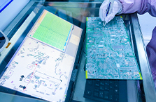
9. Quality inspection
Visual inspection: Visual inspection of PCB appearance, size, circuit continuity, etc.
Quality inspection: Monitor and check product quality at each step in the manufacturing process in real time, such as optical inspection (AOI), X-ray inspection (AXI/X-ray), etc.
Finished product testing: including electrical performance testing (ICT, FCT), functional testing and environmental reliability testing (such as thermal shock, temperature cycle, vibration testing, etc.).
Design for manufacturability (DFM) evaluation: Comprehensive evaluation of the design and manufacturing process to continuously improve the production process and reduce the defective product rate.
5.Why choose to cooperate with Xinghongtai

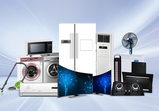
As the basic component of modern electronic equipment, the manufacturing process of PCB (Printed Circuit Board) involves multiple precise and complex process steps. With the development of miniaturization, multi-function and high performance of electronic products, higher requirements have been put forward for the manufacturing accuracy, reliability and cost-effectiveness of PCB. Therefore, it is very important to find a professional supplier.
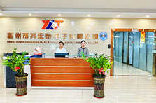
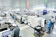
XHT has 20 years of experience in the electronic manufacturing service industry. It also has an experienced engineering design team with advanced EDA software application capabilities and a profound theoretical foundation in circuit design. Whether it is single-sided, double-sided, multi-layer, high-density interconnect (HDI) and other types of PCBs, they can provide a full range of services from conceptual design to detailed layout and routing to meet the design needs of PCBs of all types of complexity. , and ensure the excellent performance of product design in terms of signal integrity, power integrity and electromagnetic compatibility through efficient simulation optimization methods. At the same time, XHT selects high-quality substrates at home and abroad, covering diversified PCB material types such as FR-4, high Tg, halogen-free, high frequency and high speed. Based on a precise understanding of customer needs and product application environments, XHT is able to conduct customized selections on conductor materials, insulation layer materials and special functional materials to ensure a perfect match between material performance and product functions, thereby achieving the best cost performance. XHT has passed ISO9001, ISO14001, IPC-A-600/610 and other industry authoritative certifications. They promise to control product quality from the source and achieve quality tracking and control throughout the entire process. XHT aims to tailor a set of PCB design solutions for you and give you the most satisfactory service. Click here to contact us.