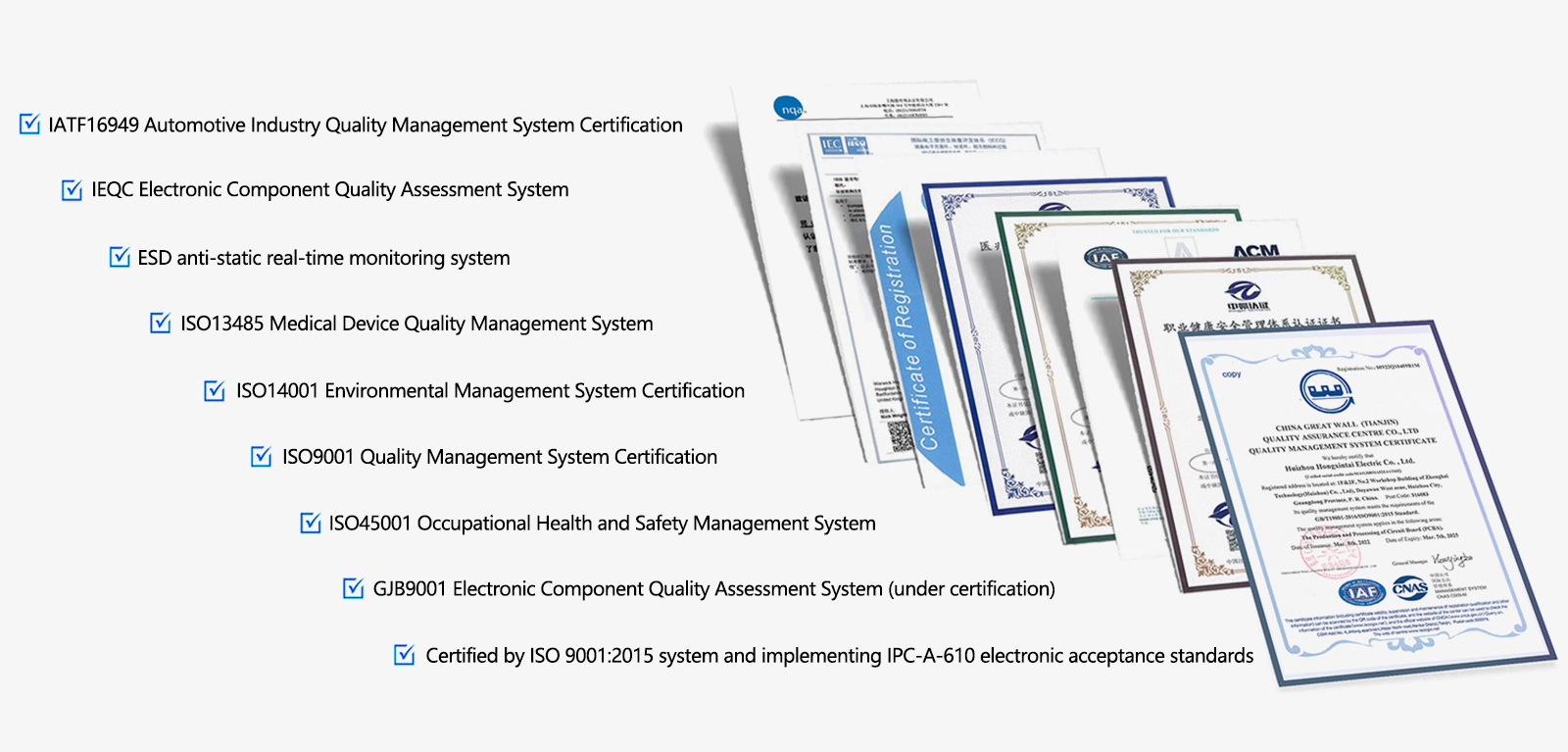
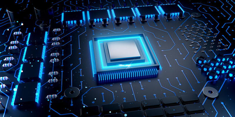
IC Packaging Technologies: PGA, BGA And LGA
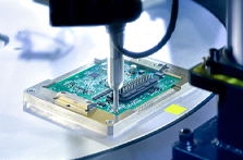
In the field of technology, packaging technology is a crucial link in chip design and manufacturing, and BGA (Ball Grid Array), PGA (Pin Grid Array) and LGA (Land Grid Array) are three representatives of this field. This article aims to analyze the advantages and differences of the three to help you choose a better product.
What is PGA?
The full name of PGA is Pin Grid Array, which is Pin Grid Array packaging. This packaging technology uses densely distributed pins all around to arrange the pins of integrated circuits into a two-dimensional matrix at a certain distance. These pins are inserted into the circuit board. The socket makes the electrical connection.
What is BGA?
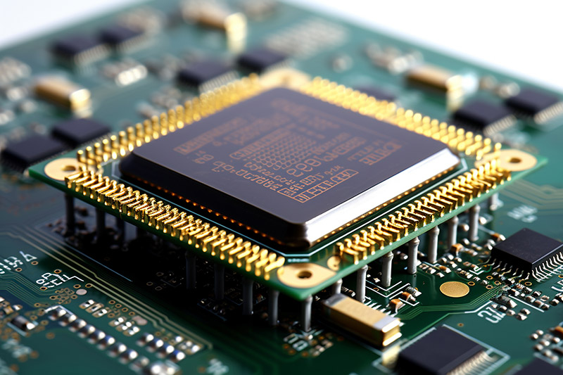
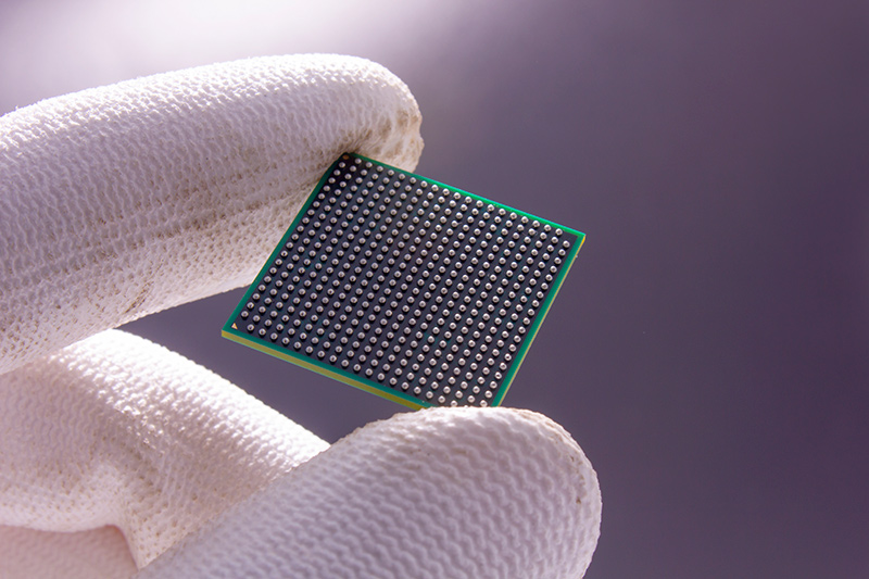
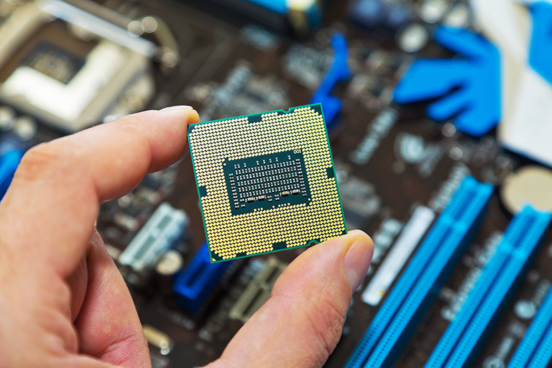
BGA, the full name is Ball Grid Array, which is ball grid array packaging technology. It is named after its unique “ball contact” layout. In this packaging method, a dense matrix of solder balls is arranged on the bottom of the chip, which is directly connected to the PCB board through reflow soldering, which significantly increases the number and density of I/O pins and effectively reduces the size of electronic products. BGA packaging is not only conducive to heat dissipation, but also because of its excellent electrical performance and high reliability.
What is LGA?
The full name of LGA is Land Grid Array, which is array grid contact packaging technology. Compared with BGA, LGA package uses a planar contact array without soldering balls. Instead, electrical connection is achieved by aligning the socket with the contact pads on the motherboard. LGA technology eliminates potential problems caused by welding, such as cold welding, voids, etc., further improving assembly quality and product life.
Advantages and Disadvantages of Three Packaging Technologies
Advantages of PGA
High pin count
Due to the matrix layout, the PGA package can carry a larger number of pins, thereby meeting the interface requirements of complex chips and improving data transmission speed and system performance.
Easy to plug and unplug
PGA-encapsulated integrated circuits can be easily plugged in or out through sockets, which facilitates the hardware upgrade, replacement and repair process and reduces maintenance costs.
Disadvantages of PGA
It takes up a lot of space
Compared with BGA or LGA packages with the same functions, PGA pins occupy extra space, making the overall package size relatively large, which is not conducive to the development of product miniaturization.
Heat dissipation capacity limitations
Although PGA has certain heat dissipation performance, its heat dissipation effect is relatively weak when faced with high-heat components such as high-performance processors.
Advantages of BGA
High density packaging
By setting a dense array of solder balls at the bottom of the chip, BGA breaks through the pin number limit of traditional packaging forms, greatly improves space utilization, allows the circuit board to accommodate more functional modules, and meets the miniaturization needs of electronic products.
Optimize signal transmission
As a connection medium, solder balls reduce the impedance of signal transmission and are conducive to high-speed data exchange. They are especially suitable for components that require fast response such as memory and graphics processors.
Improve cooling performance
Compared with traditional pin-type packaging, BGA packaging has improved thermal conductivity due to its large contact area and even distribution, which helps the chip to efficiently dissipate heat, thereby enhancing system stability and extending service life.
Simplified assembly process
Although BGA has higher requirements on welding process, once successfully completed, its leadless design can simplify the assembly process, adapt to automated production, and improve production efficiency.
This is a simple headline
Production and testing difficulty
BGA packaging requires extremely high welding precision and yield control. Especially during the rework process, the repositioning and re-soldering of solder balls is quite complicated. In addition, defective product detection also requires more advanced X-ray or three-dimensional scanning technology.
High maintenance costs
Once a failure occurs, repair work on BGA packaged devices is usually difficult and costly because the chip needs to be precisely disassembled and re-soldered.
High requirements for PCB board design
In order to achieve a perfect match with the BGA, the design of the circuit board also needs to be more precise and complex, including pad layout, circuit design, etc., which require a higher technical level.
This is a simple headline
Simplified assembly process
Since there are no physical pins, LGA packaging simplifies the assembly process and facilitates automated production, thereby reducing manufacturing costs and improving production efficiency.
Improved space utilization
After canceling the pin structure, the LGA package can accommodate more pins in the same area.
Easy maintenance: When there is a problem with the LGA packaged integrated circuit, there is no need to perform complicated desoldering operations. You only need to lightly press the control lever on the socket to easily release the fixation of the IC and achieve non-destructive uninstallation.
This is a simple headline
High docking accuracy requirements
LGA packaging has extremely high requirements for flatness and positional accuracy during assembly. A slight deviation during the docking process may cause electrical connection failure.
Thermal expansion coefficient matching problem
The coefficient of thermal expansion (CTE) between the chip and the substrate material must be well matched, otherwise stress may occur during temperature changes, leading to soldering failure or device damage.
Which packaging technology should I choose?
With the development of technology, PGA has relative disadvantages in thermal resistance and space utilization compared to BGA and LGA, and has gradually faded out in new consumer electronics products. However, there is still room for development in specific scenarios, such as test environments or some special equipment. .
BGA is often used in high-end processors, graphics cards, memories and other products with high-density packaging, excellent thermal conductivity, and miniaturization; while LGA is mostly used in CPUs and large integrated circuits that are easy to maintain, have good signal integrity, and have an impact on the production process. Higher stability situations.
Simply put, BGA has certain advantages in high-frequency signal processing and three-dimensional stacking, and is especially suitable for areas such as memory modules and graphics processors that have extremely high requirements for data transmission speeds. LGA, on the other hand, is more competitive in processors and other applications that require efficient heat dissipation and high integration due to its better thermal performance and ease of assembly.
Current status and future of IC packaging technology
With the continuous development of microelectronics technology driven by Moore’s Law, the ancient packaging technology of PGA has gradually faded out of the market, and packaging technology is also constantly evolving to meet higher performance requirements and environmental protection standards. Let XHT accompany you to witness whether the two mainstream packaging methods, BGA and LGA, can adapt to the rigorous challenges in cutting-edge fields such as 5G communications, AI computing, and autonomous driving in the future. Witness together how BGA and LGA will keep pace with the times in the future electronic packaging world, and what emerging packaging technologies are expected to become tomorrow’s stars.