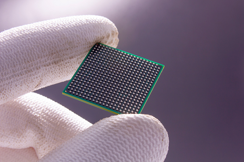


How to design PCB in limited space?
- Why should we optimize the size of PCB?
- Factors that determine PCB board size
- How to optimize PCB space utilization?
In some precision equipment, we often have the problem of insufficient PCB assembly space due to the excessive demand for internal parts. This article will help you understand and solve this problem.
Why should we optimize the size of PCB?
Optimizing the size of the PCB board has multiple implications. These reasons include the following:
Reduce costs
Optimizing PCB board size helps reduce material usage, thereby reducing production costs. During the manufacturing process, factors such as base material, production equipment, and process flow will be affected by size. By reducing size, materials can be used more efficiently and production efficiency can be improved, thus reducing costs.
Improve performance
In electronic products, PCB boards are the basis for carrying electronic components and realizing circuit connections. Optimizing the size of the PCB board can improve the performance of the circuit board, including signal integrity, power distribution, thermal design and other factors. Through reasonable layout and wiring design, signal interference and noise can be reduced, signal quality can be improved, and the overall performance of the product can be improved.
Easy to assemble and maintain
Large size PCB boards may cause difficulties in assembly and maintenance. Optimizing PCB board size allows for more reasonable space between components, allowing for easier assembly and repair processes. In addition, smaller PCB boards also mean faults are easier to identify and locate, resulting in lower repair costs and shorter downtime.
Adapt to market demand
With the development of science and technology and changes in consumer demands, electronic products are developing in the direction of miniaturization, thinness and lightness. Optimizing the size of the PCB board can make the product better adapt to market demand and meet consumer requirements for portability, aesthetics, etc.
Environmental protection
Optimizing PCB board size helps reduce waste and pollutants, making it more environmentally friendly. By reducing size, energy consumption and waste generation during production can be reduced, reducing negative impact on the environment.
Factors that determine PCB board size
Design requirements
Circuit complexity, signal integrity requirements and power distribution requirements are the basis for determining PCB board size. For example, complex circuit systems may require larger PCB boards to accommodate more components and traces.
Component layout
The layout of components has a direct impact on PCB board size. When laying out, consider component size, spacing, thermal requirements, and electrical connections to other components. Reasonable layout can minimize the size of the PCB board while meeting the electrical performance.
Number of PCB layers
The number of layers of a PCB determines its thickness. For example, a six-layer board requires a minimum thickness of 0.031 inches.
Equipment requirements
The weight and flexibility of the device also affects PCB size selection. Heavier devices may require a thicker PCB board, while devices requiring flexible circuitry (such as smart watches) may require a thinner PCB board.
How to optimize PCB space utilization?
Clarify design requirements and specifications
First of all, it is necessary to clarify the design requirements and specifications of the PCB board, including circuit complexity, number of components, heat dissipation requirements, mechanical strength, etc. These requirements and specifications will directly affect the size design of PCB boards.
Use compact components
Choosing to use components with small size and high integration can significantly reduce the size of the PCB board. For example, surface mount components (SMD) are preferred over through-hole components.
Optimize layout design
Reasonable layout design can maximize the use of PCB board space. Components should be arranged as closely as possible while maintaining sufficient spacing to ensure proper operation of the circuit. In addition, you can consider using multi-layer PCB boards to increase wiring density and thereby reduce board size.
Leverage modular design
Divide the circuit into modules, each with its own functions and interfaces. This can break down complex circuits into simpler parts for easier design, production and maintenance. At the same time, modular design can also improve the reusability and scalability of PCB boards.
Proper signal routing
Use appropriate line width and spacing to meet signal transmission needs. For example, differential lines may require special handling. Follow the 3W principle (the center distance between wires is not less than 3 times the line width) to reduce crosstalk. For high-speed signals, consider using a ground shield.
Consider production processes and costs
When optimizing PCB board size, production process and cost also need to be considered. For example, a PCB board that is too small may increase production difficulty, increase costs, or decrease reliability. Therefore, it is necessary to balance the relationship between size, process and cost while meeting design requirements.
Leverage automated design tools
Using professional PCB design software, such as AutoCAD, Altium Designer, etc., you can greatly improve design efficiency and optimize the size of the board. These software usually have automatic layout, routing, optimization and other functions, which can assist engineers in PCB design.

In summary, optimizing PCB size can not only improve the performance and stability of the circuit board, reduce manufacturing costs, improve assembly and repair efficiency, enhance scalability, but also reduce the impact on the environment. Therefore, when designing PCB, the factors of optimizing size should be fully considered to achieve better overall effect. If you have any questions about this, click here – Consult us for free
Hot Post